Korean startup’s LPU chip targets cheaper LLM inference with DRAM and Samsung 4nm backing
“The core goal is to bring AI service fees down from the current 30,000-won range to around 5,000 won.”
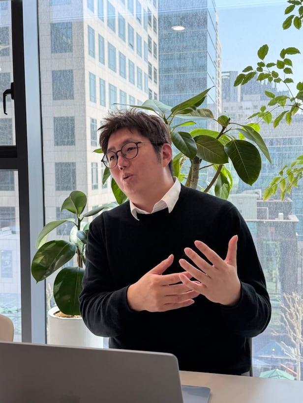
Lee Jin-won, chief technology officer (CTO) of HyperAccel, shared this blueprint in an interview with ChosunBiz at the company’s headquarters in Seocho-dong, Seoul, on Feb. 11. Even if it cannot completely replace the current AI infrastructure dominated by Nvidia graphics processing units (GPUs), the ambition is to wage a “cost-effectiveness competition” with a dedicated chip specialized for large language model (LLM) inference.
Lee is a former system semiconductor design engineer from the System LSI division at Samsung Electronics. He designed application processors (APs), the “brains” of smartphones. He joined HyperAccel as CTO in 2023 after a stint at the AI Semiconductor startup NewBula in 2021. He currently oversees AI Semiconductor architecture development.
HyperAccel is a homegrown fabless (semiconductor design) startup developing Bertha, an AI Semiconductor specialized for LLM inference (generating results). Produced on Samsung Electronics’ foundry 4-nanometer process, this chip differs from conventional GPUs in its design philosophy. The key is its proprietary architecture, the Language Processing Unit (LPU), and the use of low-cost LPDDR5X instead of expensive high-bandwidth memory (HBM).
Lee identified “memory access” as the main bottleneck for current AI Semiconductors. “It’s not that the raw compute performance is lacking and slowing things down; congestion occurs because the process of reading and writing data from memory is too complex,” Lee said. “GPUs repeatedly move data from HBM to internal SRAM and then back to the compute units, and bottlenecks appear in this process.”
HyperAccel completely changed this structure. Bertha minimizes intermediate storage (buffers) and is designed to fire data directly from external memory to the compute unit (LPU). “GPU memory bandwidth utilization is roughly around 50%, and our goal is to raise it to about 90%,” Lee said.
This architectural shift translates into “expense” innovation. For corporations running AI services today, the biggest burden is total cost of ownership (TCO), which combines equipment prices and electricity charges. “A single Nvidia H100 GPU approaches 70 million to 80 million won, and it’s not uncommon for one server to exceed 1 billion won,” Lee said. “By leveraging LPDDR to reduce both equipment costs and power consumption at the same time, our goal is to cut TCO to about one-third of GPUs.”
HyperAccel’s ambitions are not confined to data centers. It is also squarely targeting the “On-device AI” market, where devices such as home appliances and robots process AI locally. The company is working with LG Electronics on an AI accelerator for appliances, aiming to exploit Bertha’s high-efficiency architecture for real-time processing in power-constrained environments. This is currently at the proof-of-concept (PoC) stage, with ongoing collaboration for integration into future commercial products.
HyperAccel expects meaningful revenue after Bertha enters mass production. Initially, the company plans to expand supply centered on data center customers, then move into cloud providers and the On-device AI market. The following is a Q&A with Lee.
— What stage is the chip development at?
“The chip design is complete, and it is scheduled to come out this month. After validating performance and reliability in real environments, we are aiming for mass production in the second half of this year.”
— How does the LPU differ from a GPU?
“If a GPU is a ‘general-purpose accelerator’ that does a bit of everything well, an LPU is a ‘specialized architecture’ that concentrates all firepower solely on LLM inference. We optimized the chip architecture itself to the data flow of transformer models.”
— Wouldn’t using LPDDR instead of HBM be slower?
“While raw bandwidth is lower, our strategy is to raise ‘real efficiency’ by optimizing data movement paths. Thanks to that, we can serve more concurrent users on the same budget.”
— You are working with the domestic semiconductor ecosystem, including Samsung Electronics’ foundry and design houses.
“AI Semiconductor is not an industry achieved by design alone; I see it as a kind of ‘comprehensive art’ that spans foundry, design houses, packaging, and servers. In developing Bertha, we are collaborating with Samsung Electronics’ foundry and conducting design work with design houses. I believe that accumulating this experience domestically is necessary so that, in the long term, the system semiconductor ecosystem can form a virtuous cycle.”
— Who are your main customers?
“Data center operators are the core. We are already conducting a PoC with Naver Cloud and plan to expand use cases in connection with the K-Cloud project. We will demonstrate clear cost-effectiveness in specific areas.”
https://biz.chosun.com/en/en-it/2026/04/04/ULPARHKS2VAYJJJU2NMP4STYUM